

The pcb full form is printed circuit board which is an insulating board as a base material. A PCB is the backbone of any electrical device. Circuit boards are manufactured using the non conductive base board cutting it to some dimension with a conductive pattern and hole. Holes are for different purposes i.e. component holes, fasten holes, plated through holes etc. that replace the pad of electronic devices, and make an interconnection between electronic components. PCB has now become and essential component of any electronic device.
A PCB serves two purposes in the construction of an electronic device, i.e. a place to mount the components and secondly provides the means of electrical connection between the electrical components. PCB boards are designed using the latest technology that prints the conducting layers in the form of micro circuits on the main board due to this fact these circuit boards are also called printed circuit board.
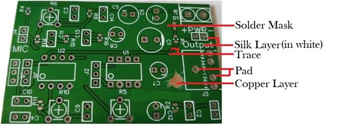
Conducting layers are typically made of thin copper foil. The board is typically coated with a solder mask that is green in color. Other colors that are normally available are blue and red. Unwanted copper is removed from the substrate after etching leaving only the desired copper traces, circuits or pathways.
Evolution of PCB
PCB were first developed during the Second World War. The revolutionary invention was made by an Austrian Engineer, Paul Eisler. Since 1929, PCBs have been mass produced for commercial applications. They were first used in transformers and capacitors.
Components of PCB Printed Circuit Board
Below is list of major components of any pcb board with brief role of each part:
- Pad: It is used for soldering plated through hole of components pin.
- Through hole: There are a via with copper and non-metal via, and metal via is used to connect the component pins between each layer.
- Mounting hole: It is used for fixing the printed circuit board.
- Wiring: To connect the electric copper film of component pins.
- Connector: To connect the components between PCB.
- Filling: It is used for copper clad of ground net so that making a great effect on reducing impedance control.
- Electric boundary: It is used for making sure PCB dimension, and the components can’t go beyond its boundary.

PCB Types & Styles
PCB are manufactured in different types and styles. The commonly available types are single sides, doubled sided and multi layers.
- Single Sided – Base material (rigid laminate with a woven glass epoxy base material) clad with copper on one side.
- Double Sided – The assembly encompasses a base material with copper on its both sides.
- Multi Layered – Encompasses several layers of substrates. Each layer is separated by an insulation.
Below are different styles which printed circuit board are available:
The most common board styles are:
- Rigid – Solid construction.
- Flex – Flexible circuits.
- Rigid-flex –Multi-circuit boards.
- Hybrid – Very small circuit. Can be integrated as part of a larger circuit.
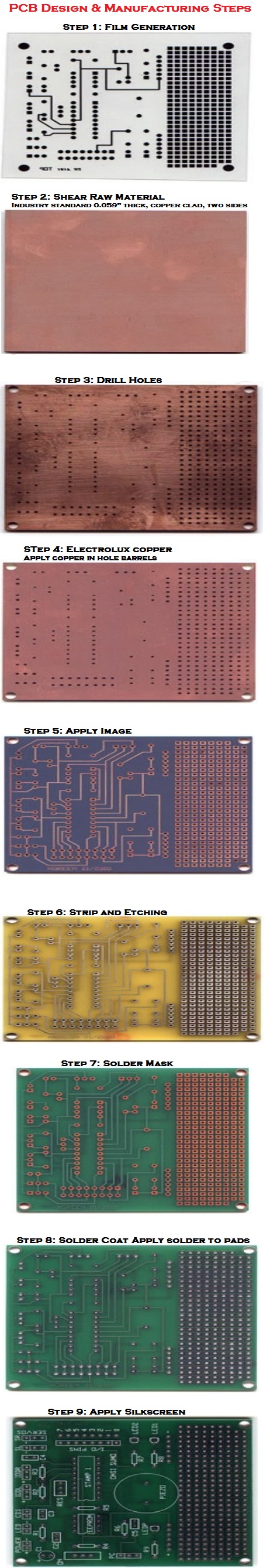
PCB Design & Manufacturing Steps
Below are the steps in PCB design and manufacturing process:
- Film Generation
- Shear Raw Material Industry standard 0.059″ thick, copper clad, two sides
- Drill Holes
- Electrolux copper Apply copper in hole barrels
- Apply Image Apply Photosensitive Material to develop selected areas from panel
- Strip and Etching: Remove dry film, then etch exposed copper. Tin protects the copper circuitry from being etched
- Solder Mask Apply solder mask area to entire board with the exception of solder pads
- Solder Coat Apply solder to pads
- Apply Silkscreen: Apply white letter marking using screen printing process

What are Parts on PCB
PCB assembly typically consists the following active and passive components.
Active components include:
- Diode – Allows current to flow in one direction.
- Transistor – Amplifies and switches electrical power and electronic signals.
- Integrated Circuits (ICs) – Responsible for several signal processing functions.
Passive components include:
- Capacitor – Stores and discharge electricity.
- Resistor – Limits the power of electrical current.
- Inductor – Responsible for creating magnetic field.

Advantages of Printed Circuit Board
The reasons why PCB is popular is that it has some special advantages as mentioned below.
High Density: For decades, high-density PCB is updated with the improvement of the integrated circuit integration and mounting technique.
High Reliability: It can make sure that PCB is great to work for a long time with a series of testing.
Design Flexibility: There are some demands for PCB properties, it can make a great effect on PCB design with standardizing design. Such as saving the time, and having high fabrication efficiently.
Scale Manufacturing ability: It can be manufactured with standardization, scale, and automation, and make sure the quality of PCB fabrication consistent by modernization management.
Test ability: Set up a great testing way and standard to test and detect the yield and shelf life of PCB.
Mountable: PCB is not only convenient to mount greatly, but also manufactures automatically and normally. What’s more, PCB and some components are mounting to the large components and machine.
Maintainability: The components are standardizing as PCB and components are designing and manufacturing greatly. So its convenient and fast to change and recover once the system is breaking down.
Applications of PCB Technology
Medical – Pacemakers, imaging equipment, drug delivery systems, wireless controllers.
Military – Weapons guidance systems, communication systems, GPS, aircraft missile-launch detectors.
Aerospace – Radar equipment, GPS, radio communication systems, control tower systems, sensors.
Telecommunication – Base stations, handheld units, communication satellites, wireless communication systems, signal processing systems.
Automotive – Electronic control module, transmission controls, LCD displays, comfort control units, air conditioning systems, music systems.
Manufacturing – Test equipment, electrical switches, industrial automation systems, control panels, industrial air conditioners, and CCTV surveillance systems.
Consumer Appliances – Oven, TV remote controllers, washing systems, lighting systems, solar power systems, UV water purifiers.